
Periodically, analysts commenting on the chip industry will pronounce that Moore’s Law is obsolete. Yet while the speed of progress is slowing down, chipmakers are still doubling the number of transistors on an integrated circuit (IC) approximately every 2.5 years. In the past, fundamentally new approaches for chip design never seemed to catch on. That’s no longer the case as fresh ideas that are essential for running some of today’s most important applications are rapidly gaining favor.
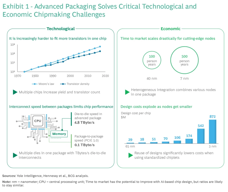
One of the most significant of these new concepts is advanced packaging, which essentially accommodates an ever-increasing number of transistors by decreasing the size of electrical contacts. Traditionally, a semiconductor chip focuses on performing one particular action or process. By comparison, an advanced multichip package incorporates multiple chips and processes into one component. This transformative approach integrates a multitude of semiconductor components into a single package, directly addressing the most critical semiconductor technical and commercial constraints. (See Exhibit 1.)
Advanced multichip packaging improves performance and time to market while reducing chip manufacturing costs and power consumption. Moreover, because it is such a radical change in chip integration, unlocking greater functionality and a reduced form factor, advanced packaging of chips is perfectly suited for key applications such as mobile devices and, in the coming years, automotive computing and generative artificial intelligence (GenAI).
For chipmakers, investors, and computing device and equipment makers, the emergence of advanced packaging represents a radical shift in the semiconductor industry landscape. The next generation of industry-leading organizations will be those that realize value creation is migrating towards companies that can design and integrate complex, system-level chip solutions using concepts like advanced packaging. Merely making individual components will rapidly lose luster, replaced by collaborative efforts that bring together the best in design, packaging, and system integration to meet the demands of the market.
Package or Perish
We are now in the “More than Moore” era. As predicted by Gordon Moore himself, it was inevitable that his law would eventually meet a threshold of diminishing economic returns. As the industry reaches the physical limitations of transistor density and chip size, the costs to cram more into a small space are exploding. But rather than try to squeeze additional transistors onto a single chip, advanced multichip packaging enables the combining of smaller, cost- and performance-optimized dies—the unpackaged semiconductor chips comprised of functional integrated circuits. It does so by using high-bandwidth interconnects and the latest front-end or wafer fabrication technologies to unleash the combined power of the packaged components. Perhaps most importantly, each of these components can have a different purpose, with computing and memory running on smaller technology nodes than components that have already reached their scaling limits, such as input/output blocks.
These components can be placed in closer proximity on advanced substrates, driving data transfer rates up to 35 times faster than the latest motherboard. This also allows for the reuse of die designs across multiple systems because the modular components can be combined in any number of ways to drive various and varied applications. By contrast, more widely used systems on a chip (SoC) are only designed for a single application.
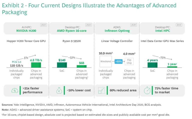
Four examples illustrate the advantages of advanced packaging. (See Exhibit 2.) The NVIDIA Hopper H200 is one of the most innovative AI core graphics processing units (GPUs) today. Six high-bandwidth memory (HBM) stacks are packaged with the central IC chips, allowing for interconnection speeds of up to 4.8 TB/s. Conventional systems, where chips are connected via a printed circuit board, are typically limited to less than 200 GB/s. Close interconnect distances also drastically decrease the power consumption of these chips, making the data centers that power large language models (LLMs) economically feasible.
The second example is the AMD Ryzen series. By opting for multiple smaller chips rather than a single large SoC, designers were able to select from a range of node sizes for each of the heterogeneously integrated dies and choose chips that were optimized for each of the package’s functions. This approach cut manufacturing costs by as much as 50%. The smaller die sizes contribute to this cost reduction by increasing fabrication yield rates because the same number of defects on a wafer is distributed across more dies.
The third illustration involves chip area size. By integrating the individual chips used in Optireg linear voltage controllers into an advanced package, Infineon was able to reduce the part’s footprint by 60%. Condensing the space required for complex systems enables a new generation of compact devices without compromising computational power or functionality. This miniaturization is key in industries where space is at a premium, such as in mobile and Internet of Things (IoT) devices, small medical equipment like hearing aids and pacemakers, and automotive computing systems.
Finally, Intel, among other integrated design manufacturers (IDMs), has greatly expanded investment in the manufacturing sides of its business to develop advanced multichip packaging capabilities. Intel has already shown that switching from a single large SoC to multiple dies in its Data Center GPU Max Series can minimize die complexity and allow existing die designs to be reused in multiple packages. In the process, Intel found that this can reduce time to market by up to 75%.
Advanced Packaging Shakes Up the Value Chain
Advanced packaging accounts for about 8% of the total semiconductor market today and is projected to double by 2030 to more than $96 billion, outpacing the rest of the chip industry. Currently, consumer electronics like smartphones dominate advanced packaging applications, but the burst of activity in the AI segment will propel future growth. AI requires rapid data exchange between computing and memory elements, which is enabled by 2.5D and 3D packaging. These approaches place more than two chips next to each other to generate high interconnect speeds at a relatively low cost. AI applications account for 25% of the total advanced packaging market already, and this is poised to grow at around 20% per year through the next decade.
As this growth trend picks up speed, advanced packaging will change the semiconductor ecosystem significantly. (See Exhibit 3.) Traditionally, the value chain of chipmaking was rather simple: one chip designer, one front-end manufacturer, and a back-end company for packaging and testing. Sometimes all these roles are handled by the same integrated device manufacturer. In this scenario, the lion’s share of value capture is concentrated in chip design and the front end—where most of the innovation lies—while packaging is relegated to a lower-margin role.
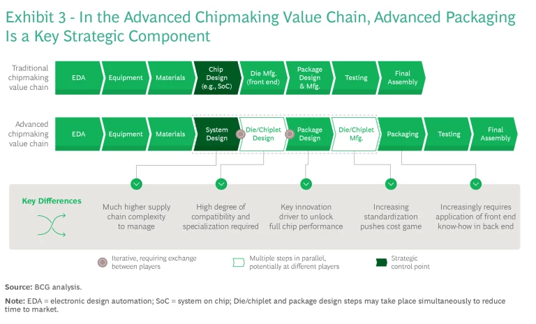
But advanced multichip packaging demands a profound rethinking of package design and how to improve it efficiently and continuously. It calls for elevated capabilities in each segment of the chip value chain. As the package becomes a core determinant of system performance, multiple semiconductor dies—often designed and manufactured by different companies—will have to be integrated in the same package, which itself is potentially produced by yet another company. As a result, system designers will need to orchestrate this new and more complex supply chain and drive close collaboration and alignment among all players.
This imminent radical alteration of the traditional chip manufacturing cycle is already prompting companies to reallocate capital expenditures and refocus R&D efforts to get out ahead of the emerging trend. In our view, the primary changes in chip industry structure will be evident in three ways:
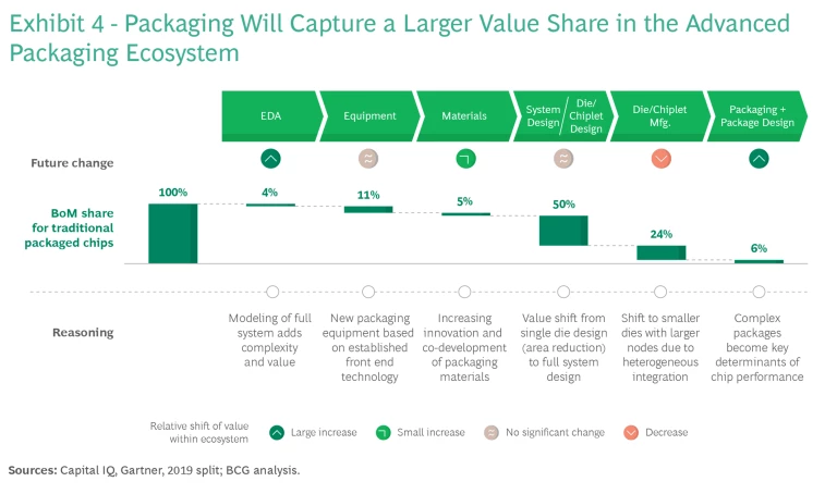
- Elevating the Role of System Design. The value share contributed by advanced package design will rise significantly, underscoring its strategic importance. (See Exhibit 4.) In response, chip designers are solidifying their grasp on this crucial segment by extending design from the single chip to the whole system, including integrating multiple dies into an advanced package.
- Shifting from Front End to Back End. The package will become a point of innovation, a differentiation driver pivotal to system performance. While front-end manufacturing will continue to command a high share of value generation, back-end design and packaging will gain in importance and profit value.
- Adapting to Complexity. Making advanced semiconductor packages is a complex process. To manage it, electronic design automation (EDA) software must be programmed to design and simulate multiple chips in a package and how their interplay may impact operating conditions, such as thermal dissipation and warpage. Similarly, materials suppliers must develop new, innovative materials to address, among other things, thermal expansion and heat transfer at the numerous interfaces in advanced packages. And packaging equipment must be modified to meet the decreasing feature sizes and increasing precision requirements of advanced packaging.
The Altered Face of the Chip Industry
As these technology changes take hold, the face of the semiconductor industry will be altered in significant ways. Chiefly, there will be a much greater degree of collaboration across chip design, package engineering, and system architecture, as each will directly impact the other. One die’s power profile will affect the next die’s thermal load and may require customized materials to optimize system performance.
Like today’s front-end landscape in which chip design and manufacturing co-evolve, strategic partnerships will increasingly extend from multiple front-end players to back-end package manufacturing. A good example of this, NVIDIA’s Hopper H100, uses a TSMC CoWoS-S package, which combines chips designed by NVIDIA and manufactured by TSMC with HBM designed and manufactured by SK Hynix. Another illustration: chip designers today work with a specific foundry’s fabrication process development kit in their electronic design automation software when building a chip. Tomorrow, this kit may contain the specific package solution in a similar manner.
Another potential area of greater collaboration will involve GenAI and machine intelligence. Integrated in EDA software, artificial intelligence capabilities can automate IC layout and floor planning; optimize power, performance, area (PPA), the essential component of semiconductor design; and simplify and expedite chip production to an unparalleled degree. But as the success of AI platforms is strongly dependent on the size and accuracy of its learning dataset, EDA software vendors and chip designers will have to balance pooling internal blueprints and frameworks to enhance the AI knowledge base without revealing their design secrets to competitors.
And even as companies jockey for position, geopolitical and regulatory constraints and opportunities will arise to affect supply chains and market access. Subsidies for advanced multichip packaging are increasingly in vogue as governments try to attract, retain, and support technology innovation in chipmaking. At the same time, since semiconductors are considered critical for national and economic security, trade barriers are being erected in various regions to protect domestic manufacturing. However, these measures could impact the availability of supplies, partners, and customers for semiconductor companies.
Strategic Solutions for Semiconductor Players
With so much change in the offing due to advanced packaging, different players in the semiconductor industry will need to adopt distinct strategic imperatives to position themselves for sustained differentiation and value capture. Here’s a breakdown of how segments of the industry can position themselves best. (See Exhibit 5.)
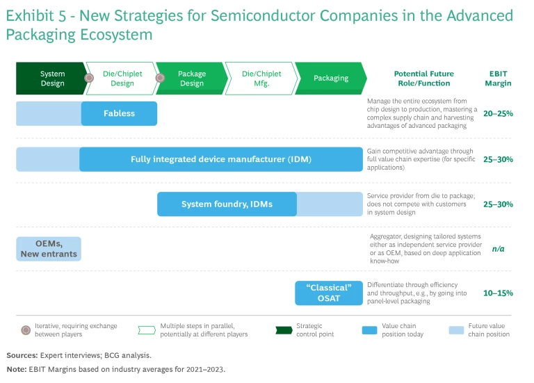
Fabless Chipmakers
Fabless chipmakers, which focus on designing chips and partner with foundries for manufacturing, will have to expand their business models quite a bit to address the challenges of advanced packaging. As the single chip becomes part of an advanced multichip package, fabless chip designers that successfully integrate the whole system development and production will capture the highest value share. However, this comes with the massive challenge of orchestrating and managing a complex supply chain across other chip designers, multiple foundries, and even material suppliers. Beyond practical execution, system designers will also be accountable to customers for the complex product’s performance, and a package manufacturer that has trusting relationships with its collaborators in this venture may be willing to take the overall liability for the system. Alternately, all involved parties in the supply chain may agree to share liabilities for a certain period after product launch when they have had enough samples to determine the most common points of failure.
Foundries
Advanced packaging will threaten revenues of leading-node foundries as it reduces demand for large monolithic SoCs, replacing them with smaller, more standardized dies. To maintain their profit levels, leading-node foundries should extend their offering into advanced packaging, positioning themselves as system foundries.
However, foundries focused on mature nodes will struggle to develop advanced packaging solutions that can directly compete with those of their leading-node peers, who are more comfortable with innovation and less hesitant to enter new markets. Those foundries can still make inroads into advanced packaging by adding to their portfolios through-silicon vias (TSVs) for silicon interposers—key ingredients that facilitate connections and communications in many advanced packages. This would allow them to increase fab utilization in times of low front-end demand for their mature chips.
Integrated Device Manufacturers
Traditionally, IDMs design, manufacture, and package their own chips, even if parts of the value chain may be outsourced. However, the economics of this business model may be challenged in an advanced packaging environment where system designers increasingly demand unpackaged dies for integration into other suppliers’ packages, limiting demand for the IDM’s packaged end product. Leading IDMs may be able to capture the system designer role themselves, particularly for lucrative, specialized applications.
Another alternative is for the IDM to offer their front- and back-end facilities to fabless customers, thereby providing systems foundry services. While that would certainly improve asset utilization, it would require strong firewalls between the IDM’s own products and those manufactured for fabless competitors that become customers. These firewalls should ensure strict separation of production lines or teams. This significantly increases complexity, but it may be imperative to create a strategy that overcomes this challenge if an IDM hopes to avoid losing its role in the chip ecosystem as advanced packaging takes hold.
Outsourced Semiconductor Assembly and Test (OSAT) Vendors
With around 30% of advanced packaging wafers already produced by IDMs and foundries, traditional OSATs must carefully assess where they best fit in a market that—even as it develops—is to a degree shifting towards other parts of the value chain. In the new packaging world, OSATs need to determine their most advantageous position between simple wire bonds and the most advanced 2.5D/3D packages.
OSATs should build on their traditional strengths of high-volume, cost-efficient manufacturing, focusing on essential packaging activities that will still be required for some time, such as bumping, in which bumps or balls of solder are spread across an entire wafer before it is diced into individual chips. And taking a more innovative approach, OSATs can develop capabilities in panel-level packaging. Dealing with large panel sizes increases the number of dies processed simultaneously and is less expensive than wafer-level packaging typically used by foundries.
In the dawn of the advanced packaging era, the landscape offers a lot of promise but also much to be wary about. Companies that recognize and invest in the strategic value of advanced packaging are setting themselves up for success. They are not only expanding their own competitive edge but are also shaping the future direction of the semiconductor industry. The winners will be companies that have successfully innovated, navigated global government policies, forged deep connections with customers and their application ecosystems, and leveraged the latest in AI and design processes.
These industry front-runners are poised to capitalize on the shift in value creation from the front end to more nuanced, complex, and value-rich back-end processes. And they are in a position to be in the sweet spot when GenAI applications—virtually all of which rely on advanced packaging components—transform from an intriguing, novel idea today to a starkly dominant platform in the coming years.
For investors, strategic partners, and semiconductor companies, the message is clear: the time to invest in and prioritize advanced packaging is now. Those that do will thrive, steering the semiconductor industry towards its next performance frontier and into a future marked by ingenuity, speed, and sustained growth.
The authors would like to thank Changwook Kim, Shreya Dwarakanath, and Jack Tu for their contributions to this article.


